光学
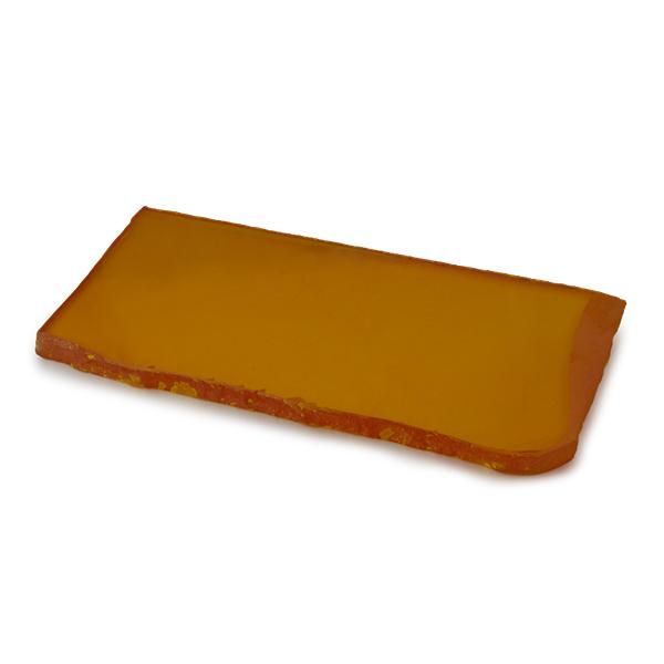
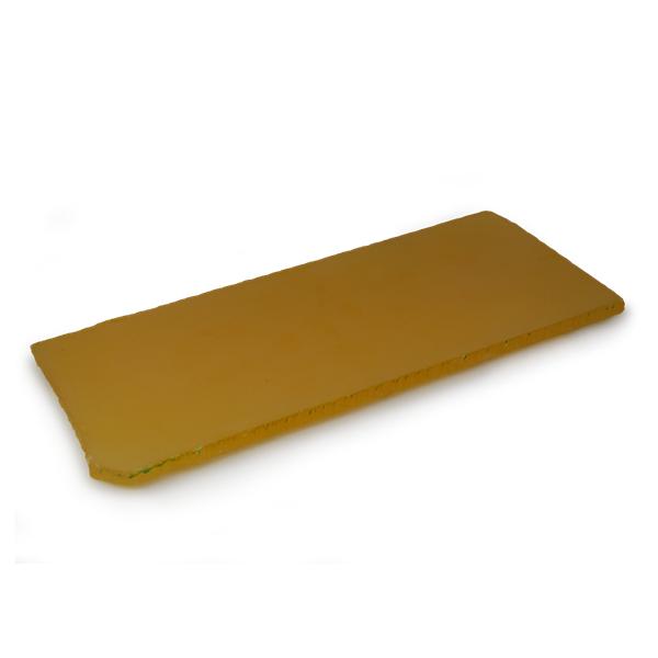
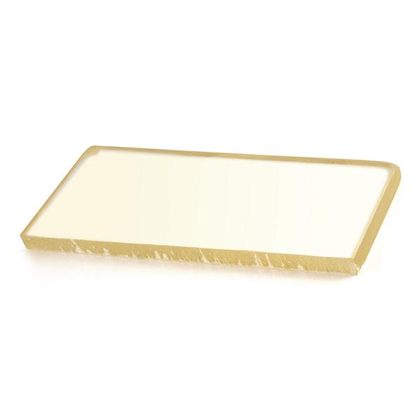
CVDダイヤモンド基板
Enjoy the benefits of diamond's unique properties – very broad transmission range, extraordinary hardness, high thermal conductivity, high resistance to thermal shock and thermal lensing, and unique electronic properties.
Coherent employs chemical vapor deposition (CVD) to grow single crystal and polycrystalline diamond in high volume, consistently producing material with low scatter, minimal absorption, and low birefringence in a wide range of cross-sectional sizes and thicknesses. Application include optics, thermal management, electronics, and quantum sensors.
CVDダイヤモンドの特性
Coherent supplies CVD diamond material in sizes up to 145 mm diameter and 2 mm thickness, and can achieve a thermal conductivity of over 2200 W/m-K.
プラズマ化学気相成長法によるダイヤモンド材料の物性 |
|
物理的特性 |
|
構造 |
多結晶または単結晶 |
粒度(多結晶) |
厚さとプロセスに依存(0.05~1 mm) |
グレード(多結晶) |
光学、熱、マイクロ波、検出器、機械、カスタム |
グレード(単結晶) |
光学、熱、マイクロ波、電子、量子、カスタム |
厚さ* |
最大2mm |
関連製品
光学製造能力
Coherent材料成長、加工、コーティング、組立までの垂直統合型体制と、厳格な品質保証(QA)についてご紹介します。これらが当社の光学部品の性能と信頼性を確保し、サプライチェーンのリスクや不確実性を最小限に抑える仕組みをご覧ください。

