材料
III-V族フォトニクスエピタキシャルウエハー
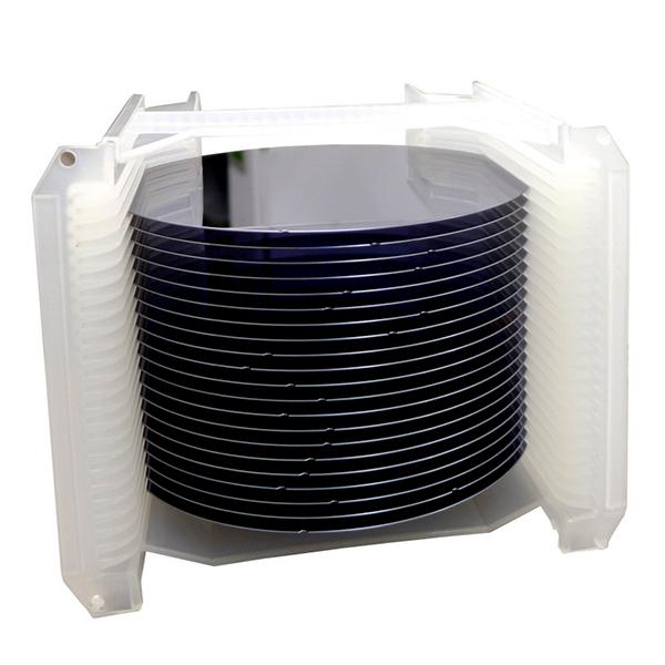
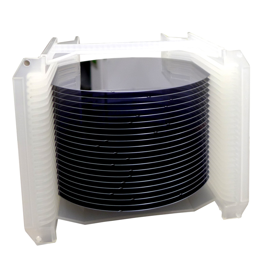
Deliver high-performance lasers, detectors, and other III-V semiconductor optoelectronic devices by fabricating with our consistent, high-quality epitaxial wafers.
The Coherent foundry employs a state-of-the-art MOCVD platform to deliver wafers which set a new standard for quality, performance, and yield. These meet the demands of challenging industrial, automotive, military, and communications applications.
III-V Photonics Wafer Capability
Source 2-inch to 6-inch wafers fabricated in our 25,000 square foot, Class 1000 cleanroom facility.
Device Type |
Base Material |
Material Capability |
Wafer Diameter |
EpiLaser® (VCSEL, EEL, LED) |
GaAs |
AlGaAs/GaAs, InGaP/GaAs, InAlGaP |
up to 150mm |
InP |
InP/InGaAs, InGaAsP, InAlAs, InAlGaAs |
up to 100mm |
|
EpiDetector® (P-i-N, APD) |
GaAs |
AlGaAs/GaAs, InGaP/GaAs |
up to 150mm |
InP |
InP/InGaAs, InGaAsP, InAlGaAs |
up to 100mm |
|
EpiSolar™ (1J, 2J, 3J, 4J) |
GaAs, Ge |
InGaP/GaAs/InGaAs, InAlGaP, AlGaAs |
up to 150mm |
InP |
InP/InGaAs, InGaAsP, InAlAs, InAlGaAs |
up to 100mm |
関連製品
注目ブログ
SiC Circuitry Makes EVs Better
Coherent is one of the few companies worldwide with a complete, vertically integrated SiC manufacturing capability. We produce SiC wafers and epitaxy, all the way through power devices and modules. Furthermore, the unmatched quality with which we can produce SiC material makes Coherent virtually the only supplier positioned to successfully transition from the current standard wafer diameter of 150 mm up to 200 mm.

注目の成功事例
Laser Framework、シーメンスのデジタルファクトリーで存在感を示す
Coherent 開発支援とCoherent FrameWorkソフトウェアにより、シーメンスはID Link製造プログラムを成功裏に導入することができました。
